viernes, 15 de mayo de 2020

Iris Recognition vs. Retina Scanning – What are the Differences?

Iris Recognition vs. Retina Scanning – What are the Differences?


In biometrics, iris and retinal scanning are known as “ocular-based” identification technologies, meaning they rely on unique physiological characteristics of the eye to identify an individual. Even though they both share part of the eye for identification purposes, these biometric modalities are quite different in how they work. Let’s take a closer look at both and then explain the similarities and differences in detail:
In biometrics, are iris recognition and retinal scanning the same thing and does the technology work the same way?
The Retina
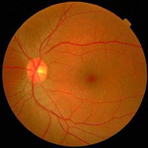
Retinal Scanning: The human retina is a thin tissue composed of neuralcells that is located in the posterior portion of the eye. Because of the complex structure of the capillaries that supply the retina with blood, each person’s retina is unique. The network of blood vessels in the retina is so complex that even identical twins do not share a similar pattern.
Although retinal patterns may be altered in cases of diabetes, glaucoma or retinal degenerative disorders, the retina typically remains unchanged from birth until death.
A biometric identifier known as a retinal scan is used to map the unique patterns of a person’s retina. The blood vessels within the retina absorb light more readily than the surrounding tissue and are easily identified with appropriate lighting. A retinal scan is performed by casting an unperceived beam of low-energy infrared light into a person’s eye as they look through the scanner’s eyepiece. This beam of light traces a standardized path on the retina. Because retinal blood vessels are more absorbent of this light than the rest of the eye, the amount of reflection varies during the scan. The pattern of variations is converted to computer code and stored in a database. Retinal scanning also has medical applications. Communicable illnesses such as AIDS, syphilis, malaria, chicken pox well as hereditary diseases like leukemia, lymphoma, and sickle cell anemia impact the eyes. Pregnancy also affects the eyes. Likewise, indications of chronic health conditions such as congestive heart failure, atherosclerosis, and cholesterol issues first appear in the eyes.
What is iris scan? Iris recognition and retinal scanning are two different biometric identification technologies
The Iris
Iris Scanning: The iris (plural: irides or irises) is a thin, circular structure in the eye, responsible for controlling the diameter and size of the pupils and thus the amount of light reaching the retina. “Eye color” is the color of the iris, which can be green, blue, or brown. In some cases it can be hazel (a combination of light brown, green and gold), grey, violet, or even pink. In response to the amount of light entering the eye, muscles attached to the iris expand or contract the aperture at the center of the iris, known as the pupil. The larger the pupil, the more light can enter. Iris recognition is an automated method of biometric identification that uses mathematical pattern-recognition techniques on video images of the irides of an individual’s eyes, whose complex random patterns are unique and can be seen from some distance.
Unlike retina scanning, iris recognition uses camera technology with subtle infrared illumination to acquire images of the detail-rich, intricate structures of the iris. Digital templates encoded from these patterns by mathematical and statistical algorithms allow unambiguous positive identification of an individual. Databases of enrolled templates are searched by matcher engines at speeds measured in the millions of templates per second per (single-core) CPU, and with infinitesimally small False Match rates. Hundreds of millions of persons in countries around the world have been enrolled in iris recognition systems, for convenience purposes such as passport-free automated border-crossings, and some national ID systems based on this technology are being deployed. A key advantage of iris recognition, besides its speed of matching and its extreme resistance to False Matches, is the stability of the iris as an internal, protected, yet externally visible organ of the eye.
Similarities and Differences: While both iris and retina scanning are ocular based biometric technologies, there are distinct similarities and differences that differentiate the two modalities. Iris Recognition uses a camera, which is similar to any digital camera, to capture an image of the Iris. The Iris is the colored ring around the pupil of the eye and is the only internal organ visible from outside the body. This allows for a non-intrusive method of capturing an image since you can simply take a picture of the iris from a distance of 3 to 10 inches away.
Retinal Scanning requires a very close encounter with a scanning device that sends a beam of light deep inside the eye to capture an image of the Retina. Since the Retina is located on the back of the eye, retinal scanning was not widely accepted due to the intrusive process required to capture an image.
Here is an overview of some similarities and differences between the two modalities:
Similarities:
  • Low occurrence of false positives
  • Extremely low (almost 0%) false negative rates
  • Highly reliable because no two people have the same iris or retinal pattern
  • Speedy results: Identity of the subject is verified very quickly
  • The capillaries in the iris and retina decompose too rapidly to use a amputated eye to gain access

Differences:

  • Retinal scan measurement accuracy can be affected by disease; iris fine texture remains remarkably stable
  • An iris scan is no different than taking a normal photograph of a person and can be performed at a distance; for retinal scanning the eye must be brought very close to an eyepiece (like looking into a microscope)
  • Iris scanning is more widely accepted as a commercial modality than retinal scanning
  • Retinal scanning is considered to be invasive, iris is not

Chart: Iris vs. Retinal Scanning: What are the similarities and differences?

Biometric Modality
Iris
Retina
Category
Extremely fastand reliable search results
xx
Uses safe, low energy-infrared light for scanning (same as what is used in TV remote controls)
Uses a digital camera to capture the image
x
Has absolutely no negative impact on human health
x
Ability to save biometric images for auditing purposes
xx
Ideal for large databases
xx
Completely contactless
xx
Measurement accuracy affected by disease
x
Requires close proximity to camera for successful scan
x
Works with all ages – no patient re-enrollment required
xx

lunes, 27 de enero de 2014

smart contact lens project

Esto sí es Progreso

You’ve probably heard that diabetes is a huge and growing problem—affecting one in every 19 people on the planet. But you may not be familiar with the daily struggle that many people with diabetes face as they try to keep their blood sugar levels under control. Uncontrolled blood sugar puts people at risk for a range of dangerous complications, some short-term and others longer term, including damage to the eyes, kidneys and heart. A friend of ours told us she worries about her mom, who once passed out from low blood sugar and drove her car off the road. 

Many people I’ve talked to say managing their diabetes is like having a part-time job. Glucose levels change frequently with normal activity like exercising or eating or even sweating. Sudden spikes or precipitous drops are dangerous and not uncommon, requiring round-the-clock monitoring. Although some people wear glucose monitors with a glucose sensor embedded under their skin, all people with diabetes must still prick their finger and test drops of blood throughout the day. It’s disruptive, and it’s painful. And, as a result, many people with diabetes check their blood glucose less often than they should. 

Over the years, many scientists have investigated various body fluids—such as tears—in the hopes of finding an easier way for people to track their glucose levels. But as you can imagine, tears are hard to collect and study. At Google[x], we wondered if miniaturized electronics—think: chips and sensors so small they look like bits of glitter, and an antenna thinner than a human hair—might be a way to crack the mystery of tear glucose and measure it with greater accuracy.
We’re now testing a smart contact lens that’s built to measure glucose levels in tears using a tiny wireless chip and miniaturized glucose sensor that are embedded between two layers of soft contact lens material. We’re testing prototypes that can generate a reading once per second. We’re also investigating the potential for this to serve as an early warning for the wearer, so we’re exploring integrating tiny LED lights that could light up to indicate that glucose levels have crossed above or below certain thresholds. It’s still early days for this technology, but we’ve completed multiple clinical research studies which are helping to refine our prototype. We hope this could someday lead to a new way for people with diabetes to manage their disease.

We’re in discussions with the FDA, but there’s still a lot more work to do to turn this technology into a system that people can use. We’re not going to do this alone: we plan to look for partners who are experts in bringing products like this to market. These partners will use our technology for a smart contact lens and develop apps that would make the measurements available to the wearer and their doctor. We’ve always said that we’d seek out projects that seem a bit speculative or strange, and at a time when the International Diabetes Federation (PDF) is declaring that the world is “losing the battle” against diabetes, we thought this project was worth a shot. 


Introducing our smart contact lens project


viernes, 15 de junio de 2012

El final de los tres Transbordadores Discovery, Endeavour y Atlantis de la NASA

El final de los tres Transbordadores Discovery, Endeavour y Atlantis de la NASA


Actualizado en Abril 2012 sobre la entrada original: http://alfe2000.blogspot.com.es/2007/07/nasa-la-parte-negra-hacia-abajo.html

Al cerrar el programa espacial, se han recogido los tres transbordadores Discovery, Endeavour y Atlantis. Aquí lo vemos en el aeropuerto Dulles:

Detach Orbiter

Y aquí en vuelo:

Fly to Destination
De la web de la NASA:

"The final chapter is about to close on NASA's 30-year space shuttle program.
The agency's three remaining space-flown orbiters — Discovery, Endeavour and Atlantis — each made their last flights in 2011, and are now being prepped for retired life in museums. Discovery has been gifted to the Smithsonian National Air and Space Museum's Stephen F. Udvar-Hazy Center in Chantilly, Va., while Endeavour is bound for the California Science Center in Los Angeles.
Atlantis is due to stay close to home at the Kennedy Space Center Visitors Complex in Cape Canaveral, Fla. Additionally, the prototype orbiter Enterprise, which never flew to space, moved to New York City's Intrepid Sea, Air and Space Museum. Enterprise previously resided at the Smithsonian."

domingo, 7 de diciembre de 2008

Lo que puede dar de sí un buen "par"

Como curiosidad, el servicio ADSL, puede funcionar correctamente con uno solo de los dos hilos del “par” de cobre que nos llega desde la centralita de la compañía telefónica, en cambio el servicio de teléfono clásico, necesita obligatoriamente los dos hilos del par.

Es por esto que hay veces que el teléfono no funciona, pero en cambio, el ADSL va perfectamente, en este caso se nos ha podido desconectar o romper uno de los hilos del par, y si coincide que es el que no usa ADSL, pues no nos funcionará el teléfono y sí el ADSL.

Es más, hay productos como el “Catena CNX-5 Broadband DSL” que permiten a los operadores de telefonía ofrecer a sus clientes, a través de un “par” de cobre, dos líneas de teléfono clásico y dos conexiones ADSL.

A finales del 2007, con 29 años, el Dr John Papandriopoulos (foto), de la Universidad de Melbourne, ha desarrollado y patentado una tecnología (SCALE/SCAPE) que permite llegar hasta 250 Megabits por segundo, sin necesidad de alterar el “par” de cobre en uso. Actualmente la tecnología aplicada al ADSL ofrece 1Mb/s y alcanza 20Mb/s con ADSL2+, siempre en teoría.

Ya está trabajando en USA, junto con el padre del ADSL, el Professor John Cioffi de la Stanford University, quien ya tiene diseñado un sistema para llevar datos a 1-2Gb por segundo sobre el mismo “par” de cobre, pero su aplicación práctica tardará todavía unos años.

Su web actual en la que comenta más detalles: http://jpap.org

y Apple le compra su compañía Snappylabs:

http://techcrunch.com/2014/01/04/snappylabs/

viernes, 16 de mayo de 2008

¿Por qué en un CD caben 74 minutos de sonido?


El CD fué inventado en el laboratorio de física de Philips (Philips Natuurkundig Laboratorium) en Eindhoven, financiado por un equipo conjunto de Philips (60%, parte óptica y mecánica) y Sony (40%, parte de corrección de errores). El primer CD comercial fue producido el 17 de Agosto de 1982 en la fábrica de Polygram en Hannover, (Alemania).


La historia popular dice que Akio Morita, el fundador de Sony, especificó que el tamaño debía ser de 74 minutos, para alojar la Novena Sinfonía de Beethoven, pero...


...La realidad es menos romántica:


El tamaño físico del CD viene dado en la especificación original como la dimensión de la diagonal de la cinta de cassette redondeado al número par. Como la cinta tiene 11,6cm, el redondeo fue a 12cm. Entonces debido a la tecnología existente y teniendo en cuenta diversos factores como la frecuencia de muestreo, corrección de errores y densidad óptica disponible, resultaba que podía alojar 74 minutos.

Es más, en la especificación original, y debido a que en la época había gran interés por el sonido cuadrofónico, se reservó un bit para indicar grabación de 4 canales, reduciendo en este caso el tiempo a la mitad. Hoy en día éste bit todavía se mantiene sin uso.

lunes, 17 de marzo de 2008

¡Que cosa más curiosa !


Contador de rayos beta y gamma Radex

Es curioso ver que por ejemplo en el interior del Monasterio de El Escorial no sube de 0,26 µSv/h, y estamos rodeados de granito. En cambio en el exterior del nuevo Teatro Auditorio de San Lorenzo alcanza valores más elevados, debido al tipo de piedra utilizada en el recubrimiento.


El pasado viernes 18 vine en AVE desde Barcelona a Madrid, y pasa cerca de la central de Ascó donde hubo un escape recientemente. Comprobé que dentro del tren en todo su recorrido no subió de 0,13 µSv/h.


En cambio al sacar el lector del bolsillo en la estación de Atocha, marcaba 0,48µSv/h.


Seguiremos informando.


Después del desatre de Fukushima en Japón, podemos ver este tipo de instrumentos en uso por Greenpeace entre otros, como ejemplo la foto con una medida de 7,68µSv/h.


miércoles, 1 de agosto de 2007

Intel presenta Polaris, su Chip con 80 cores


detail Meet Polaris - it's the North Star, y'know
By Charlie Demerjian: domingo 11 febrero 2007, 19:52
THE ROADMAP to high end chips is now more than ever dominated by interconnects and the ability to get data in, out and around the chip.
Couple that with a trend toward more task specific CPUs and you have a new "paradigm" in the works. Those paradigms are shown off in Intel's Polaris chip.
Polaris was the 80 core CPU shown off at the last IDF as a demo for teraflop computing on a chip. To put this in perspective, an ACM article (1) estimated that in 1988, it could be done in 100 megawatts, but chips like the 68882 could drop that by a notable amount. They theorised that five megawatts was possible including cooling with some advances in tech.
The first one that was actually built was ASCI Red at Sandia National Lab. It was 104 cabinets housing 10,000 Pentium Pros and spread out over 2500 square feet. It consumed a mere 500kw, yay progress. Polaris does this 10 years later in 275 square mm and consumes 62W when doing so.

As you can see, part Polaris is made up of tiles, identical tiles, 80 of them in an 8 * 10 arrangement. Each tile does not do very much, this is a test chip, not a general purpose CPU. The core has two FP engines, data and instruction memory and a router. The main point of this chip is the router to test mesh interconnects..


When you have a chip capable of more than a teraflop, you need a way to get the data to feed it on and off the chip. The router is a 6 port unit that will shuffle a mere 80GB/s around with a 1.25ns latency. If you consider that the chip has 80 of these, it can send a lot of bits to and fro, and that is the point of Polaris. At 3.16 GHz, the bisection bandwidth of the chip is 1.62 Tbps. The router can send data to it's neighbors in each of the four directions as well as up to the stacked memory that Intel won't talk about yet. The last link goes to the core itself.

The routing algorithm used isn't all that complex, it is just a simple wormhole setup. You make a path between routers, send the data down, and close the link, it is a virtual pipe. This simplicity is one of the ways they can get the latency so low.
The main point of Polaris is just that, to route data around, but there are other things tested here, power savings and potentially disparate cores. Power savings is nothing new, but when you have a router on the core that needs low latency, it can get tricky. In the sleep modes, the FPs can save 90% of peak power, memory can cut back over 50% but the router can only drop down 10%. Latency does not play well with sleep modes.
That brings us to the future, as in why should we care about a test chip that can hit a somewhat arbitrary number of calculations? The answer is twofold, this is two of the next big things for Intel on one chip, and will be a third as soon as they talk about the stacked memory.
The first is the whole idea of asymmetric cores. If you have a mesh that can shuffle data around willy nilly, you don't need the same things at all nodes. The nodes are independent of the IO functionality, so as long as they have the right interface and understand the protocols, you can put anything you want on a tile.
Right now, you have two FP units, a couple of chunks of ram and a little control circuitry. Replace that with a full x86 CPU and you start to see the possibilities. Replace half of them with x86 CPUs, a quarter with GPUs, toss in a physics co-processor and few other things and you start to see the point.
With a mesh base and a tiled set of chips, you can tailor CPUs to almost any need you want. You can also make the same architecture have 5, 20 or 100 tiles, Celeron, Core Number Numeral and Xeon, all nice and tidy. Easy to design, manufacture and customize.
The other bit is the mesh itself. Computing has gone from shared busses to point to point interconnects like HT. On die, and sometimes off die, you have switches and crossbar interconnects to get the data around. Those devices don't scale all that well, nor do ring busses when you are talking about hundreds of cores instead of a few.
That is where meshes come in, they will take Intel from a cap in the tens of cores to potentially hundreds or thousands. Polaris is about flexibility as well as expandability. It also is a very obvious pointer as to where Intel is going at the end of the decade and beyond.
In the end, Polaris doesn't really do all that much from a functional perspective. It can calculate a teraflop, but that isn't all that useful in the real world. Expect a next gen Polaris to be much more functional in the general sense, followed by things you can buy with meshes. µ
(1) Frey, A. H. and Fox G. C. "Problems and Approaches for a Teraflop Processor", Proceedings of the third conference on Hypercube concurrent computers and applications: Architecture, software, computer systems, and general issues - Volume 1, 1988